High-Efficiency SWIR Imaging
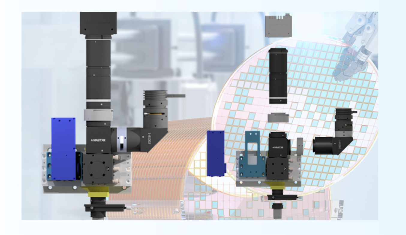
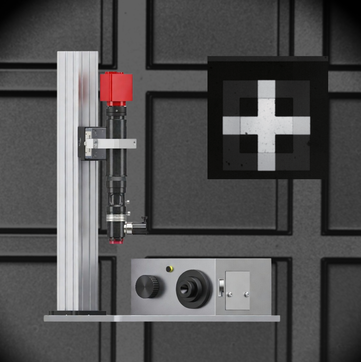
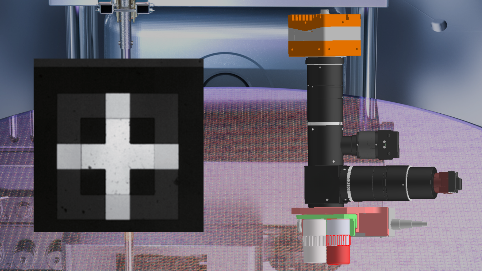
For special imaging requirements of wafers, SiC, semiconductor packaging, and other materials, matching appropriate optical systems and SWIR cameras enhances the contrast of defects and structural features and improves inspection efficiency.
Broadband Coating Options
VIS/VNIR/SWIR coating options cover the NIR/SWIR 400–1500 nm range, meeting imaging requirements for different materials and inspection targets.
Balanced Resolution and Field of View
Magnification and NA are matched according to camera pixels, sensor size, and inspection targets. This preserves micrometer- and even sub-micrometer-level detail while optimizing inspection efficiency.
Multiple Imaging Modes
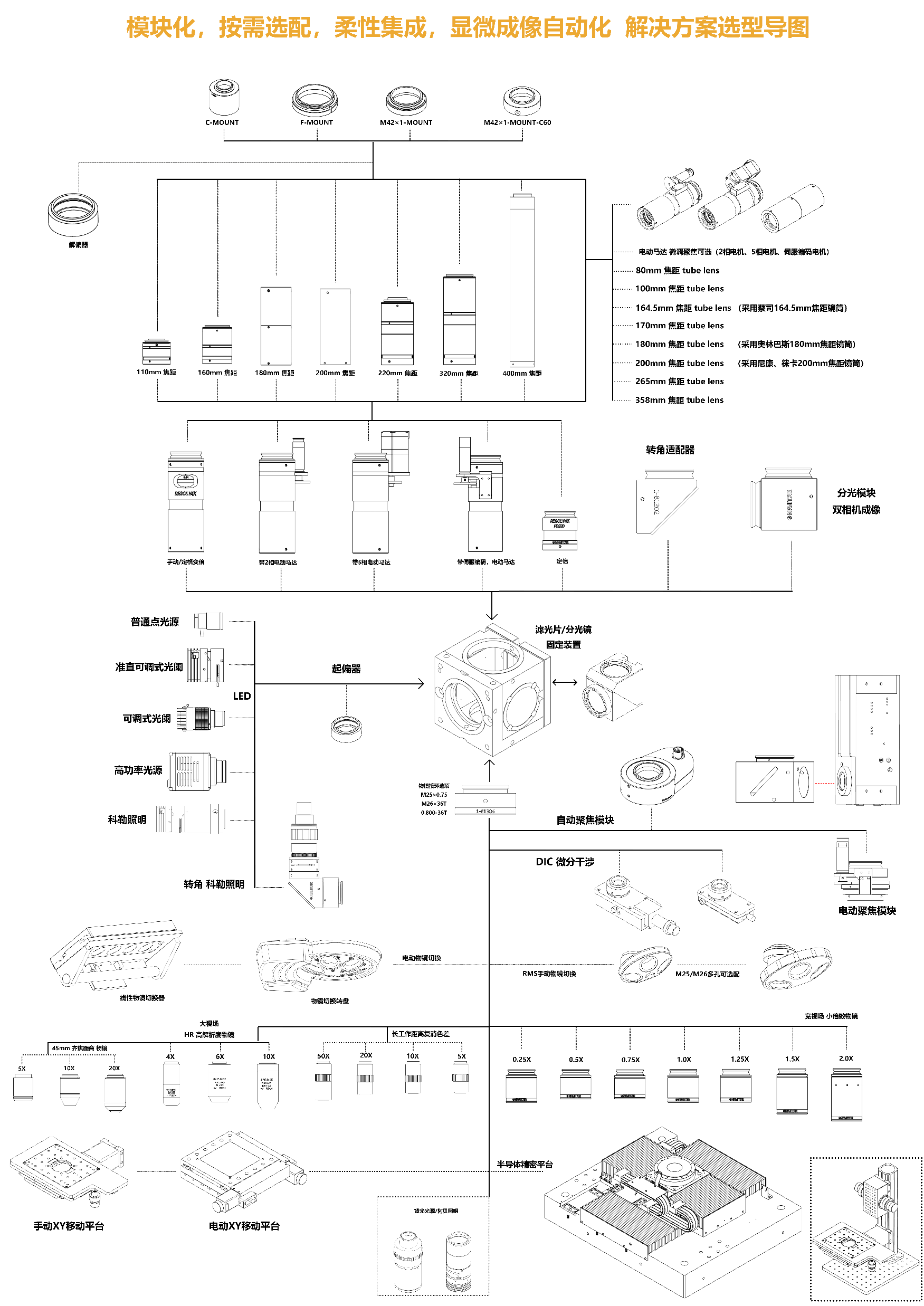
Fixed magnification, manual continuous zoom, and motorized continuous zoom are supported, allowing flexible switching between rapid localization over a large field of view and local high-resolution observation according to inspection needs.