For semiconductor AOI tasks, “seeing” is no longer the threshold. The bigger challenge is achieving higher efficiency and higher precision at the same time: large-field, high-throughput inspection on one side, and micron or even sub-micron defect resolution on the other. Traditional microscopy solutions often struggle to do both well.
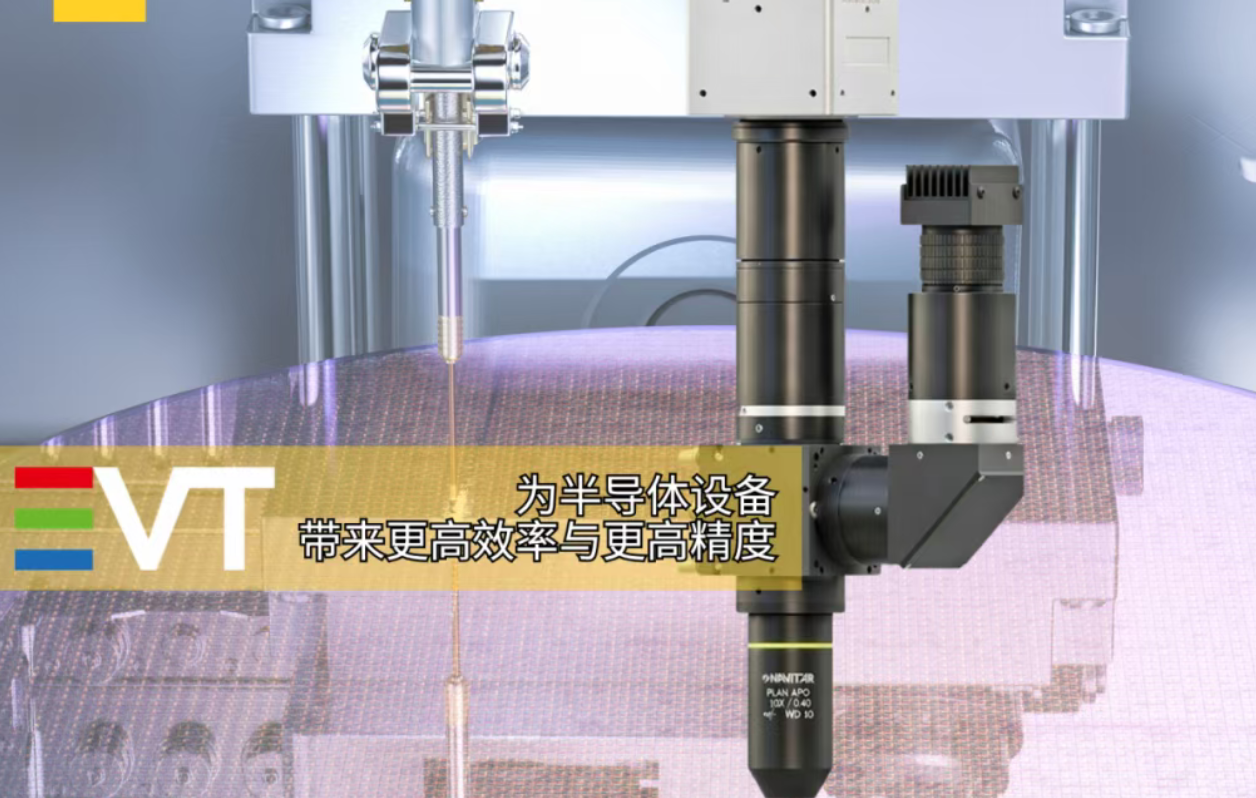
- Balancing Field of View and Resolution: higher magnification improves resolution but reduces throughput.
- Adaptation Conflict Between Multiple Scenarios and Fixed Configurations: different materials, processes, and defect types have very different optical requirements.
- High Engineering Cost: each new requirement may mean re-adjusting the optical path, validating, and integrating again.
As a result, equipment can be built, but it is difficult to iterate efficiently over time.
The EVT team’s approach is straightforward: rather than making one “optimal configuration,” we build a system that can continuously approach the optimum. Based on Navitar’s modular microscopy architecture, we developed a flexible microscopic opto-mechanical system for AOI.
It can be freely configured for different inspection tasks, dynamically balancing efficiency and precision while reducing integration and debugging complexity. Essentially, it turns an optical design problem into an engineering configuration problem.
The system structure is built around four basic units and expandable capabilities. The core functions of the entire AOI microscopic opto-mechanical system rely on the collaboration of these four modules.
1. Imaging Tube Lens
Resolution is not simply magnification; it is a matching relationship. Many system problems are not caused by poor lenses, but by mismatch between the lens and the camera.
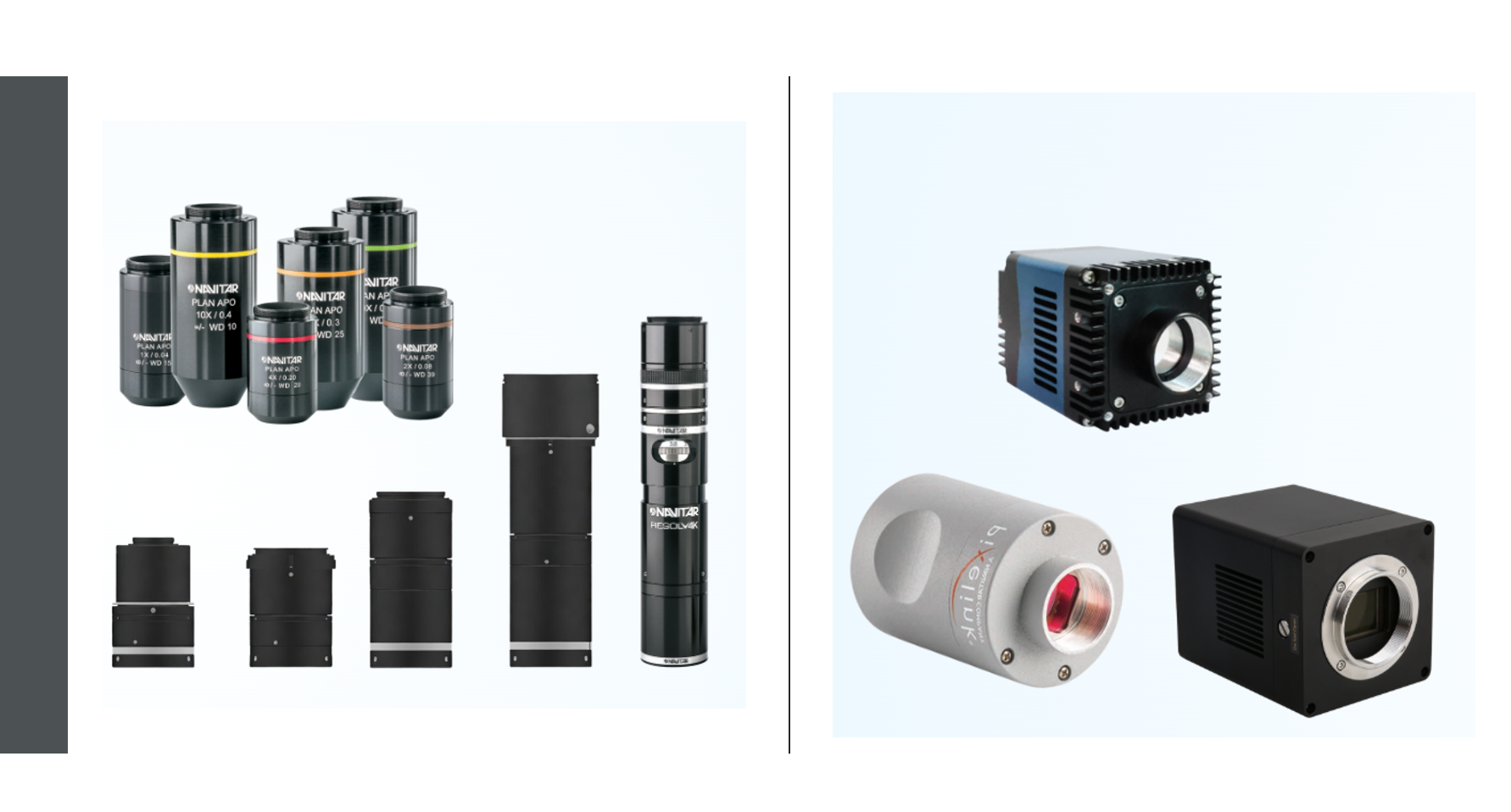
In microscopy imaging, the objective (NA + wavelength) determines theoretical resolution, while camera pixel size determines whether those details can be sampled. If they do not match, under-sampling can lose details, while over-sampling creates redundant data and slows system efficiency.
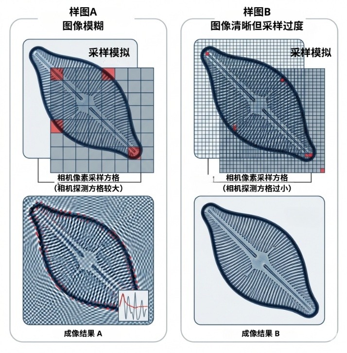
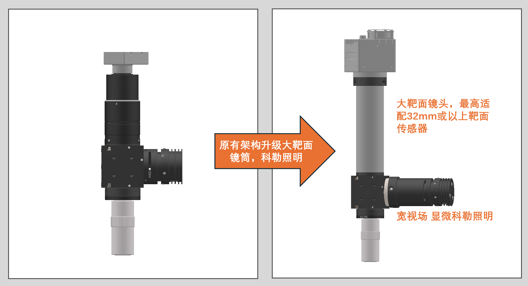
We provide multi-magnification apochromatic microscope tube lenses compatible with cameras of different pixel sizes and sensor formats. At the sample plane, they help match effective pixel size with the resolution limit, aligning with Navitar’s concept of high-throughput apochromatic tube lenses matched to large-format detectors and fully releasing the inspection potential of the optical system.
2. Microscopic Illumination
For AOI equipment, uniformity is not just about looking good; it affects algorithm cost. In AOI scenarios, many issues are caused not by invisibility but by inconsistent imaging across areas. Non-uniform illumination causes grayscale drift, unstable thresholds, and repeated algorithm tuning, slowing debugging and reducing stability.
We recommend a standardized Köhler illumination system with reflected and transmitted modes. Through multi-stage aperture control and conjugate-plane adjustment, it achieves uniform illumination from center to edge and a stable, reproducible light-field distribution.
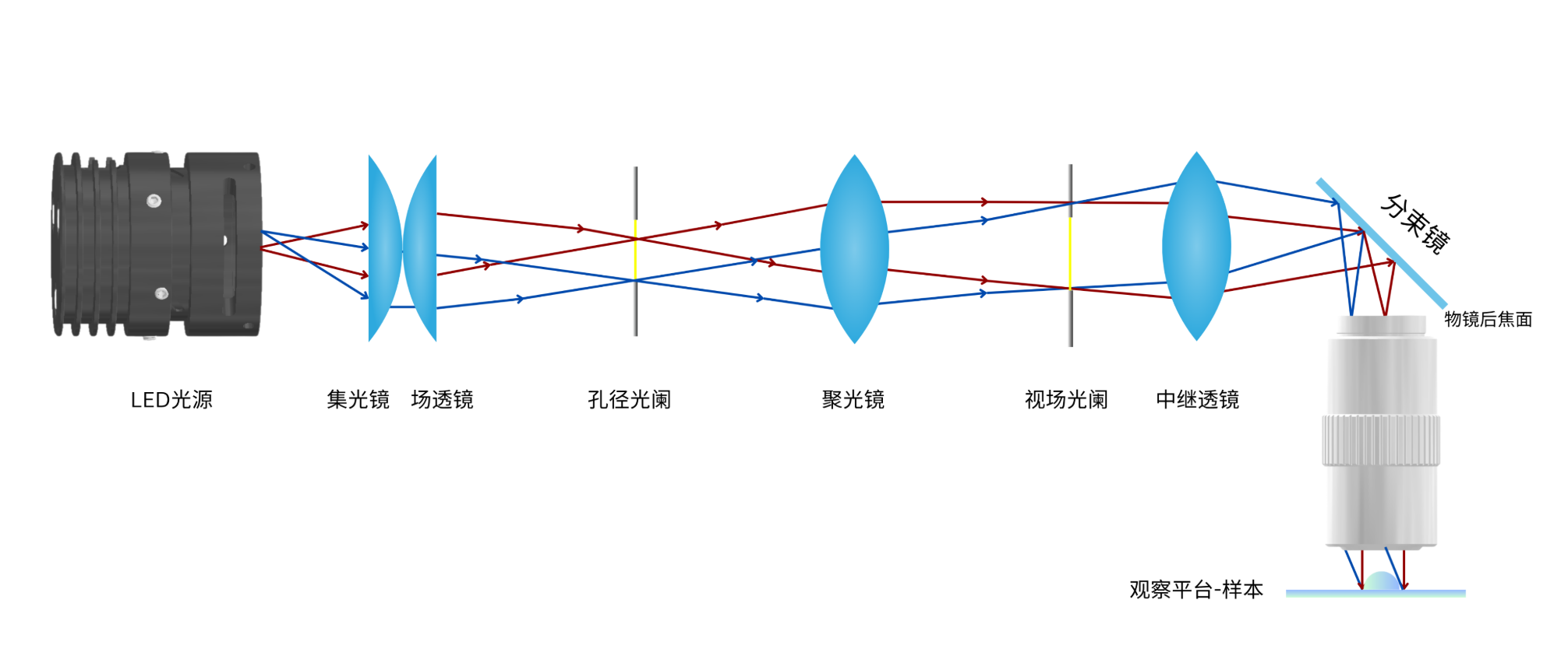
This system can be directly embedded into AOI equipment as a standardized module without additional complex illumination design, while supporting customized wavelengths for special inspection scenarios.
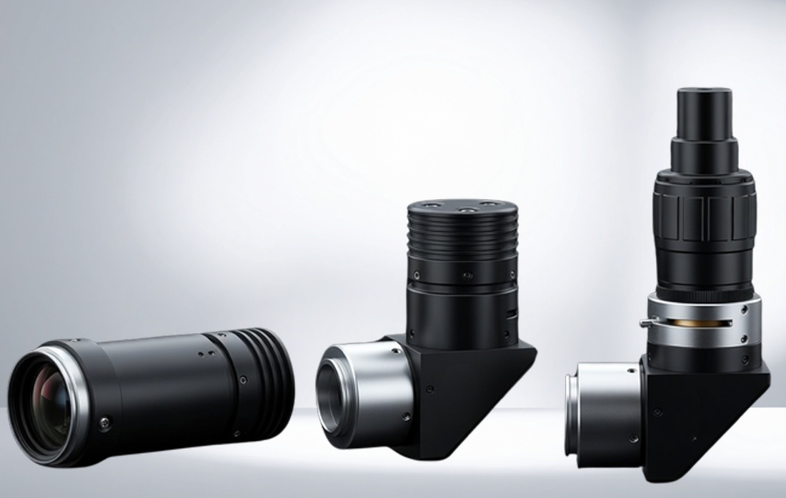
3. Microscope Objectives
The key is to select an objective suited to the application. Different AOI scenarios require different objective strategies. Based on diverse semiconductor inspection needs, we optimize objective selection for both industrial stability and inspection suitability.
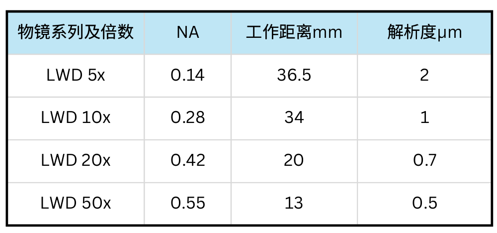
Long Working Distance Objective: provides different coatings from NUV to NIR, magnification from 1X to 100X, NA up to 0.7, and working distances from 6 to 36.5 mm, suitable for mechanically constrained equipment spaces such as package internal inspection and large wafer stages.
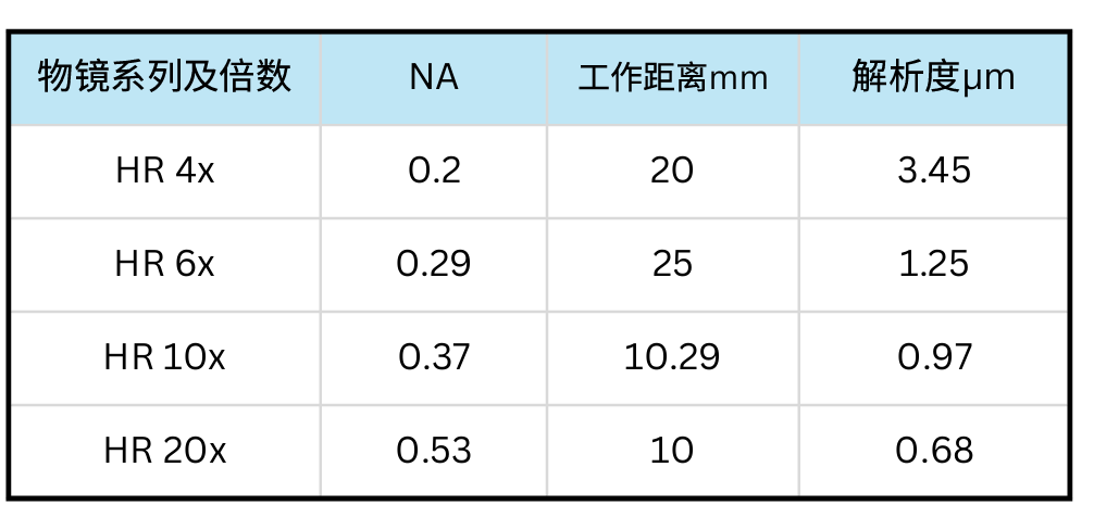
High-Resolution Objectives (HR Series): fills the 4× / 6× magnification gap with resolution close to traditional 5× / 10× options, balancing efficiency and precision while reducing unnecessary magnification redundancy and data-processing pressure.
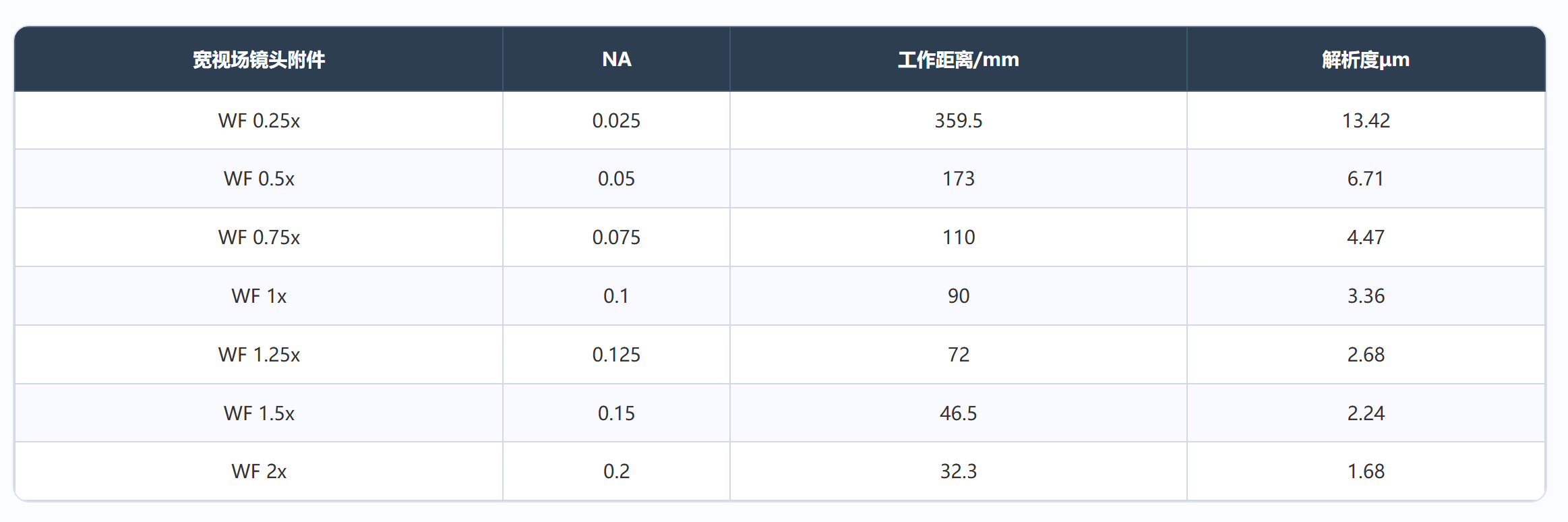
Wide-Field Objectives: offers a field of view up to 110 mm and resolution around 1.68 μm, suitable for rapid whole-wafer scanning while combining large-area inspection with micro-defect recognition.
4. Expandable Functional Modules
Different defect types, material properties, and inspection precision requirements cannot be fully covered by basic imaging modules alone. Therefore, we provide expandable functional modules that can be seamlessly integrated into infinity-corrected optical paths, enabling online system upgrades without rebuilding the original architecture.
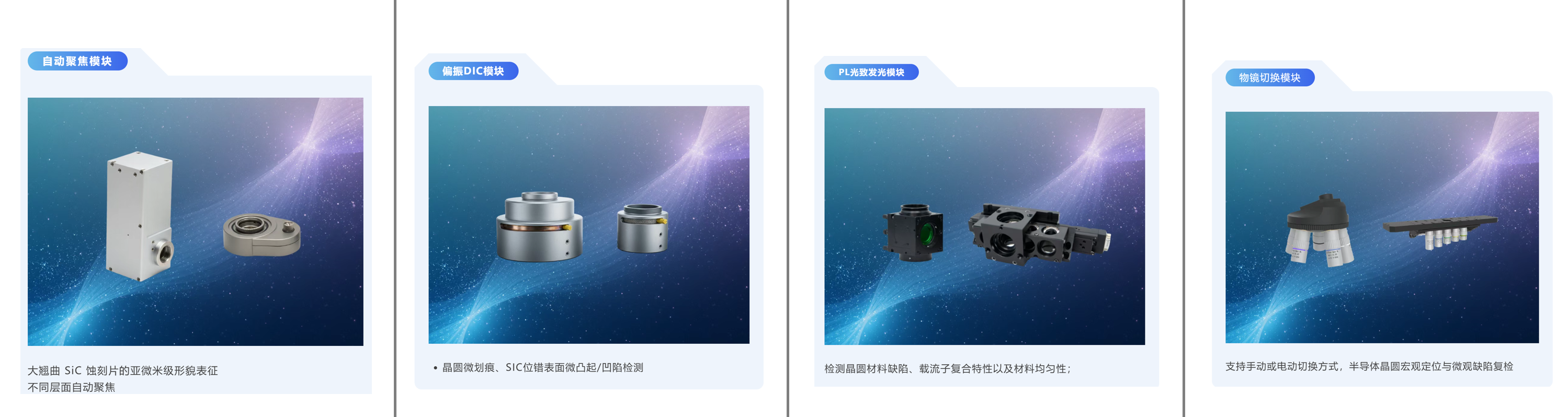
The core value of integration is reducing repeated system rebuilding. In real equipment development, each new requirement can mean redesigning an optical system—changing cameras, adapting to new processes, and adjusting inspection precision—often requiring optical redesign, repeated validation, and debugging. This consumes time and slows equipment iteration.
A modular architecture changes this significantly: one system can cover multiple inspection tasks, and local module replacement can adapt to new cameras and processes without rebuilding the optical path.
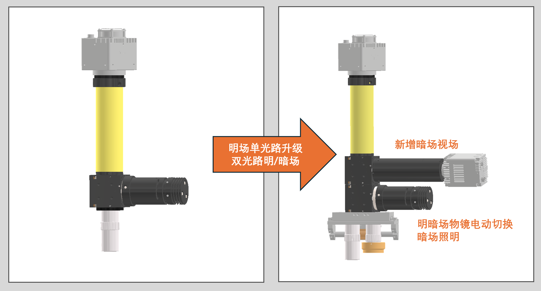
Dark field enhances scattering signals from tiny particles and scratches, while bright field stably captures surface morphology and contamination information. Dual optical paths can switch seamlessly, expanding defect detection capability without changing the main architecture.
In AOI scenarios, system usability and iteration capability are often as important as optical performance.
If you are developing AOI equipment, please contact us for optical inspection system integration or microscopy imaging solution optimization, turning imaging challenges into more controllable engineering problems.